
From DIP to Chiplet:
The Material Innovation Logic Behind Semiconductor Packaging Evolution, Earlysun Technology's Perspective
🔬 Chip Packaging · Tech Iteration · Material Empowerment
Every breakthrough in the semiconductor industry relies on the collaborative iteration of the entire "Design-Manufacturing-Packaging" chain. If chip design is "defining performance" and manufacturing is "realizing potential", then packaging is "releasing value"—it not only determines the physical form and application adaptability of the chip but also directly affects signal transmission efficiency, heat dissipation capability, and long-term reliability.
From early DIP insertion packaging to today's Chiplet packaging, the core demand of technological evolution has always centered on "smaller, faster, more reliable", and behind all these changes is the support of packaging material innovation.
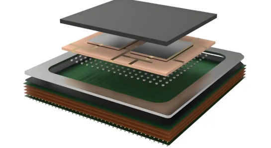
I. Semiconductor Packaging Evolution: From "Simple Wrapping" to "System Integration"
The development of semiconductor packaging technology is essentially a continuous response to chip integration and application needs, which can be roughly divided into three key stages:
1. Traditional Packaging: Core of "Mechanical Protection + Basic Interconnection"
Early technologies like DIP, SOP, QFP had the core goal of physical connection and mechanical protection. Solder joint spacing was loose (usually ≥0.5mm), and the core requirement for materials was "strong compatibility, mature process".
2. Advanced Packaging: Core of "High Density Interconnection + Miniaturization"
Technologies like FlipChip, BGA, CSP emerged. Solder joint spacing shrank to 0.3~0.5mm, placing "high precision, low defect" requirements on materials: solder paste needs finer powder particle size, and underfill needs high fluidity.
3. Frontier Packaging: Core of "System Integration + High Performance"
Chiplet and 3D IC have become hot spots. Packaging has upgraded to "multi-chip system integration", with solder joint spacing shrinking to the micron level. Materials need: high-density interconnection capability, extremely low coefficient of thermal expansion (CTE), and excellent heat dissipation performance.

II. Scenario-based Material Innovation: Earlysun Technology's "Packaging Adaptation Scheme"
The differences in core requirements of different packaging technologies dictate that material innovation must "suit the remedy to the case". Based on a deep understanding of packaging technology evolution, Earlysun Technology has targetedly developed a full series of packaging materials:
🏗️ Traditional Packaging Scenario: Stable and Reliable "Basic Guarantee"
For processes like DIP and QFP, Earlysun Technology's general-purpose high-compatibility solder paste and packaging epoxy resin have core advantages of "strong process adaptability and stable performance". Packaging epoxy resin has good fluidity and curing shrinkage rate, ensuring long-term stable operation of chips in conventional environments.
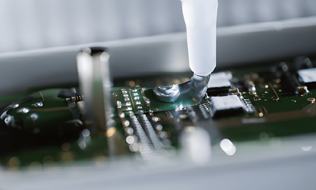
🚀 Advanced Packaging Scenario: Precise Breakthrough "Performance Upgrade"
Low CTE Underfill targets thermal stress problems in flip chips, using a modified epoxy resin formula with a coefficient of thermal expansion (CTE) as low as 15ppm/℃ or less. Highly matched with the thermal expansion characteristics of chips and substrates, it effectively absorbs stress generated during temperature cycling, reducing solder joint fracture risk by over 80%.
As the semiconductor industry moves into the "Post-Moore Era", technologies like Chiplet, 3D IC, and hybrid bonding will become mainstream directions in the packaging field.
Earlysun Technology will continue to increase R&D investment in frontier packaging materials, keeping up with the pace of technology iteration. From traditional to advanced packaging, Earlysun Technology's material innovation always centers on "empowering the industry", continuing to use technological innovation as an engine to contribute Chinese material strength to the high-quality development of the global semiconductor industry.